Silikon karbür substratın işlenmesi zor olsa da, elektronik bileşenlerde tek kristal silisyum karbür uygulamasının gelecekteki gelişim yönü haline gelmesi ve böylece silisyum karbür cihazlarının büyük ölçekli uygulama ve tanıtım olmasını sağlamak için, zor silisyum karbür işleme problemini çözmenin bir yolunu bulmak gereklidir.
Şu anda, SiC malzeme işleme teknolojisi temel olarak aşağıdaki işlemlere sahiptir: yönlü kesme, talaş kaba taşlama, ince taşlama, mekanik parlatma ve kimyasal mekanik parlatma (ince parlatma). Bunların arasında kimyasal-mekanik parlatma son işlemdir ve işlem yöntemi seçimi, işlem rotası düzenlemesi ve işlem parametresi optimizasyonu, parlatma verimliliğini ve işlem maliyetini doğrudan etkiler.
Ancak SiC malzemelerin yüksek sertliği ve kimyasal stabilitesi nedeniyle geleneksel CMP cilalama işleminde talaş kaldırma oranı düşüktür. Bu nedenle endüstri, plazma destekli, katalizör destekli, ultraviyole destekli ve elektrik alanı destekli dahil olmak üzere düzleştirme ultra hassas işleme teknolojisini destekleyen yardımcı verimlilik teknolojisini aşağıdaki şekilde incelemeye başladı:
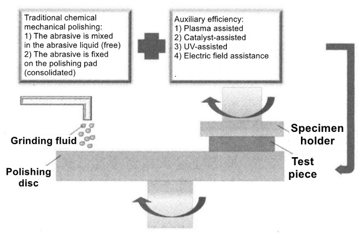
01 Plazma destekli teknoloji
YAMAMURA Kazuy ve ark. ilk olarak, yüzey malzemelerini plazma yoluyla daha yumuşak bir oksit tabakasına oksitleyen ve aynı zamanda aşındırıcı sürtünme ve aşınma yoluyla malzemeleri ortadan kaldıran yardımcı bir kimyasal-mekanik cilalama olan plazma destekli cilalama (PAP) işlemini önerdi.
Temel prensip şudur: RF jeneratörü reaksiyon gazı (su buharı, O, vb. gibi) aracılığıyla, serbest grupların güçlü oksidasyon kapasitesine sahip serbest gruplar (OH serbest grupları, O serbest radikaller gibi) içeren bir plazma üretmek. SiC malzeme oksidasyon modifikasyonunun yüzeyi. Yumuşak bir oksit tabakası elde edilir ve daha sonra yumuşak aşındırıcılarla (CeO2, Al2O3 vb.) parlatılarak oksit tabakası kaldırılır, böylece SiC malzemenin yüzeyi atom seviyesinde pürüzsüz bir yüzeye ulaşır. Ancak PAP süreci test ekipmanının yüksek fiyatı ve işleme maliyetleri nedeniyle, PAP süreci işleme SiC çiplerinin tanıtımı da sınırlıdır.
02 Katalizör destekli süreç
Endüstriyel alanda, SiC kristal malzemelerin yüksek verimli, ultra hassas işleme teknolojisini keşfetmek amacıyla araştırmacılar, katalitik destekli kimyasal-mekanik parlatma için reaktifler kullanıyor. Malzeme gidermenin temel mekanizması, reaktiflerin katalizi altında SiC yüzeyinde yumuşak oksit tabakasının oluşması ve oksit tabakasının aşındırıcının mekanik olarak uzaklaştırılmasıyla çıkarılmasıdır. Yüksek kaliteli bir yüzey için. Literatürde, aşındırıcı olarak W0.5 elmas ile kimyasal mekanik parlatma teknolojisinin geliştirilmesine yardımcı olmak için Fe3O4 katalizörü ve H2O2 oksitleyici kullanılmıştır. Optimizasyondan sonra 12,0 mg/saat parlatma hızında Ra=2,0 ~ 2,5 nm yüzey pürüzlülüğü elde edildi.
03 UV destekli teknoloji
SiC yüzey düzleştirme işleme teknolojisini geliştirmek için. Bazı araştırmacılar kimyasal-mekanik cilalama işleminde katalize yardımcı olmak için ultraviyole radyasyonu kullandılar. UV fotokatalitik reaksiyon güçlü oksidasyon reaksiyonlarından biridir. Temel prensibi, UV ışığının etkisi altında fotokatalist ve elektron yakalayıcı arasındaki fotokatalitik reaksiyonla aktif serbest radikaller (·OH) üretmektir.
OH serbest gruplarının güçlü oksidasyonu nedeniyle. Oksidasyon reaksiyonu, daha yumuşak bir SiO2 oksit tabakası (MOE sertliği 7'dir) oluşturmak için SiC yüzey tabakasında meydana gelir ve yumuşatılmış SiO2 oksit tabakasının aşındırıcı cilalama ile çıkarılması daha kolaydır; Öte yandan oksit tabakası ile levha yüzeyi arasındaki bağlanma mukavemeti, SiC levhanın iç bağlanma mukavemetinden daha düşüktür, bu da parlatma işleminde aşındırıcının kesme kuvvetini azaltır, yüzeyde kalan çizik derinliğini azaltır. gofretin yüzeyini iyileştirir ve yüzey işleme kalitesini artırır.
04 Elektrik alanı destekli teknoloji
SiC malzemelerinin uzaklaştırılma oranını arttırmak için bazı araştırmacılar elektrokimyasal mekanik parlatma (ECMP) teknolojisini önermişlerdir. Temel prensip şudur: Geleneksel kimyasal mekanik parlatma işleminde parlatma sıvısına doğru akım elektrik alanı uygulanarak, elektrokimyasal oksidasyon altında SiC parlatma yüzeyinde oksidasyon katmanı oluşturulur ve oksit katmanının sertliği önemli ölçüde azalır. Verimli, ultra hassas işleme elde etmek amacıyla yumuşatılmış oksit katmanını çıkarmak için aşındırıcı kullanılır. Ancak şunu da belirtmek gerekir ki, anot akımı zayıfsa işleme yüzeyi kalitesi daha iyi olur ancak talaş kaldırma oranı çok fazla değişmez; Anot akımı güçlüyse malzeme kaldırma oranı önemli ölçüde artar. Ancak çok güçlü anot akımı, daha düşük yüzey doğruluğuna ve gözenekliliğe yol açacaktır.
Kısacası, kimyasal-mekanik parlatma, SiC malzemeleri için hala en potansiyel düzleştirme ultra hassas işleme yöntemidir, ancak yüksek kaliteli SiC levhaları daha verimli bir şekilde elde etmek için yukarıda belirtilen yardımcı işlemler potansiyel seçeneklerdir. Ancak ilgili çalışmaların olmaması nedeniyle SiC malzemeleri üzerindeki etkisi hala tahmin edilememektedir. Bu nedenle, ilgili yardımcı proseslerin kimyasal-mekanik cilalama teknolojisi üzerindeki etkisini derinlemesine inceleyebilirsek ve kimyasal-mekanik cilalama yardımcı verimlilik arttırma teknolojisinin işleme mekanizmasını nicel ve nitel araştırma araçlarıyla daha fazla ortaya çıkarabilirsek, bunun gerçekleştirilmesi büyük önem taşıyacaktır. SiC malzemelerinin sanayileşme uygulaması ve tanıtımı.